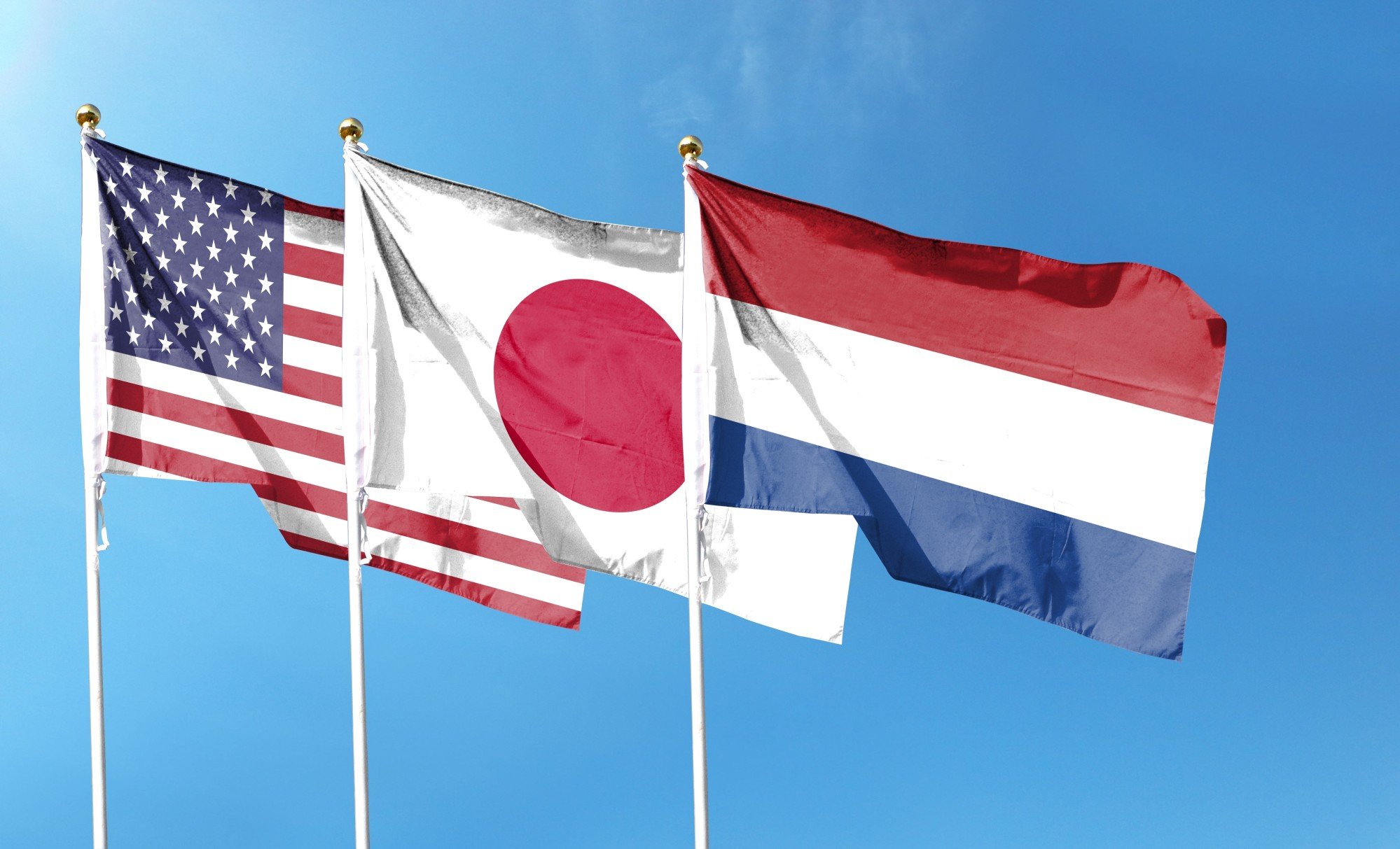
Tech war: US-Japan-Netherlands alliance triggers debate over scale of its possible impact on China’s semiconductor industry
- Chinese Foreign Ministry spokesman Mao Ning said the US-led export control pact threatens the stability of the global semiconductor supply chain
- Before export controls come into effect, lithography machine supplier ASML said its details must first be drawn up and implemented into legislation
Details of that pact, however, remain unknown. There is no plan for a public announcement of the restrictions, and actual implementation could take months as Tokyo and Amsterdam finalise legal arrangements, according to the report.
Chinese Foreign Ministry spokeswoman Mao Ning said on Monday at a briefing that the US-led agreement is not only harmful to all concerned parties, but threatens the stability of the global semiconductor supply chain.

Commercial chip manufacturing using 28-nm process machinery started in 2011. 28-nm chips are used on a wide range of applications, including central processing units, graphics processors, high-speed networking chips, and integrated circuits that power smartphones, tablets and other consumer electronics devices.
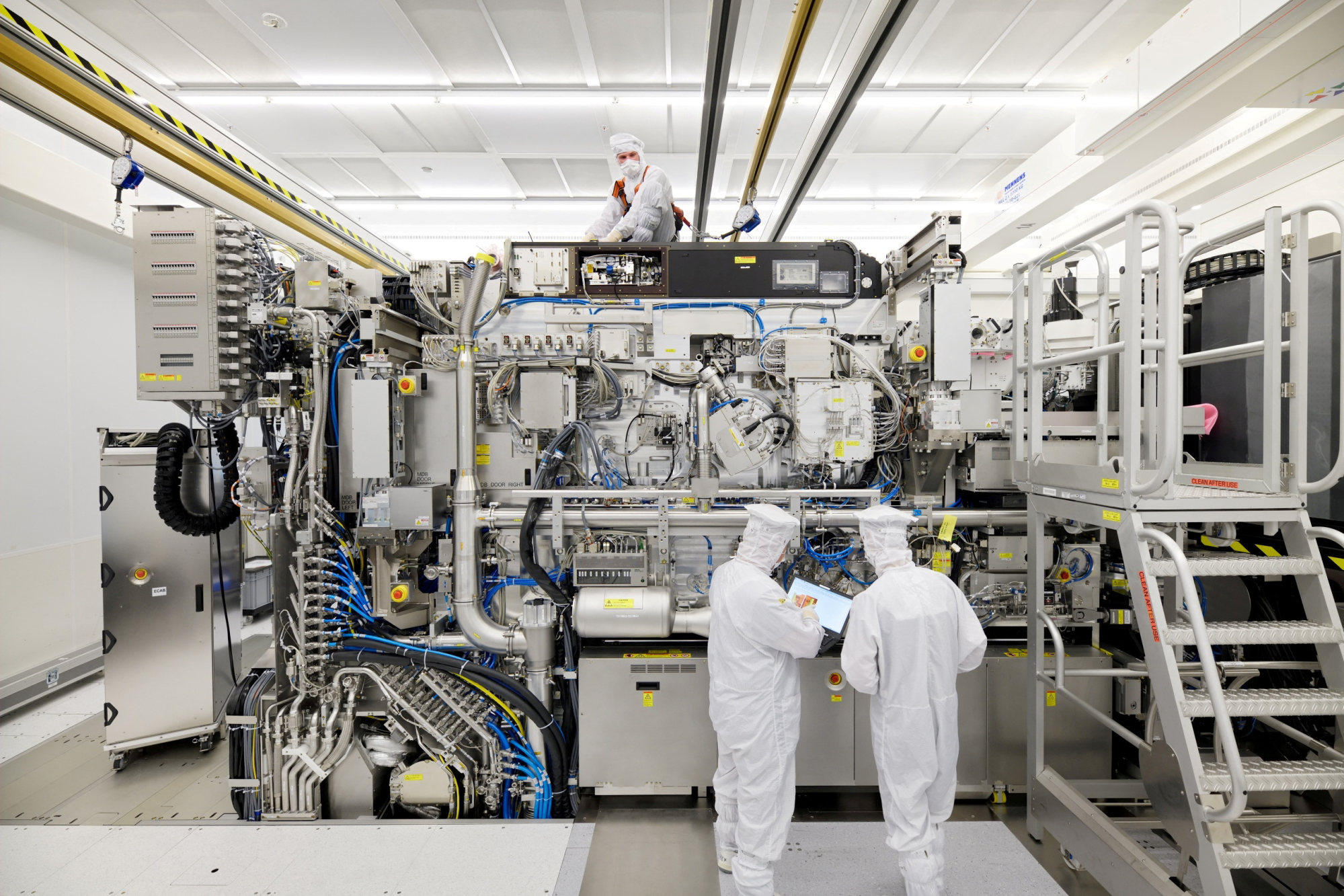
So-called ultraviolet lithography equipment, which uses laser technology to basically carve a pre-designed circuit onto a wafer, is at the centre of the joint export control pact, according to a report authored by Jefferies analyst Edison Lee on Monday.
EU joins US in ‘depriving China of the most advanced chips’, official says
ASML confirmed in a statement on Sunday that the scope of agreed export controls could go beyond advanced lithography technology. Before export controls come into effect, “it has to be detailed out and implemented into legislation which will take time”, the company said.
Alternative lithography equipment vendors are Japan’s Nikon Corp and Canon, which make less-advanced deep ultraviolet (DUV) systems. There are several versions of DUV, and the most advanced one is called ArF Immersion DUV, which enables chip technology processing nodes between 45-nm and 7-nm.

He indicated that if the ban applies only to 14-nm or below chip-processing technology, “it may be hard to enforce since tracking what the machine is used for over time is challenging”.
Echoing that comment, Nicolas Gaudois, head of Asia-Pacific technology research at UBS, said: “It is quite hard for the equipment companies to show that the equipment being shipped is actually not [falling] in the scope of [restrictions].”
China’s Hua Hong to focus on mature chip nodes with new US$6.7 billion wafer fab
“We believe the lack of official announcements and details could mean that Japan and the Netherlands have agreed only in principle, but not yet to the details,” Jefferies Lee said. “The biggest sticking point is likely what kind of lithographic machine should be restricted.”
Further restrictions on DUV equipment could limit China’s output in mature chip technologies, according to Arisa Liu, a senior semiconductor research fellow at the Taiwan Institute of Economic Research.
Still, China’s imports of lithographic machines rose to about US$4 billion in 2022, up from US$1.3 billion in 2017, according to the Jefferies report. It said import statistics show that China has increasingly relied on Japanese vendors, with lithographic machine imports from them growing to 33 per cent in last year from 27 per cent in 2017.


